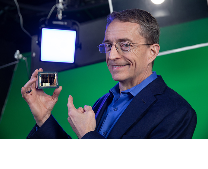
Intel CEO Pat Gelsinger outlined the company’s path forward to manufacture, design and deliver leadership products and create long-term value for stakeholders. During the company’s global “Intel Unleashed: Engineering the Future” webcast, Gelsinger shared his vision for “IDM 2.0,” a major evolution of Intel’s integrated device manufacturing (IDM) model. Gelsinger announced significant manufacturing expansion plans, starting with an estimated $20 billion investment to build two new factories (or “fabs”) in Arizona. He also announced Intel’s plans to become a major provider of foundry capacity in the U.S. and Europe to serve customers globally.
“We are setting a course for a new era of innovation and product leadership at Intel,” said Gelsinger. “Intel is the only company with the depth and breadth of software, silicon and platforms, packaging, and process with at-scale manufacturing customers can depend on for their next-generation innovations. IDM 2.0 is an elegant strategy that only Intel can deliver – and it’s a winning formula. We will use it to design the best products and manufacture them in the best way possible for every category we compete in.”
IDM 2.0 represents the combination of three components that will enable the company to drive sustained technology and product leadership:
- Intel’s global, internal factory network for at-scale manufacturing is a key competitive advantage that enables product optimization, improved economics and supply resilience. Gelsinger re-affirmed the company’s expectation to continue manufacturing the majority of its products internally. The company’s 7nm development is progressing well, driven by increased use of extreme ultraviolet lithography (EUV) in a rearchitected, simplified process flow. Intel expects to tape in the compute tile for its first 7nm client CPU (code-named “Meteor Lake”) in the second quarter of this year. In addition to process innovation, Intel’s leadership in packaging technology is an important differentiator that enables the combination of multiple IPs or “tiles” to deliver uniquely tailored products that meet diverse customer requirements in a world of pervasive computing.
- Expanded use of third-party foundry capacity. Intel expects to build on its existing relationships with third-party foundries, which manufacture a range of Intel technology – from communications and connectivity to graphics and chipsets. Gelsinger said he expects Intel’s engagement with third-party foundries to grow and to include manufacturing for a range of modular tiles on advanced process technologies, including products at the core of Intel’s computing offerings for both client and data center segments beginning in 2023. This will provide the increased flexibility and scale needed to optimize Intel’s roadmaps for cost, performance, schedule and supply, giving the company a unique competitive advantage.
- Building a world-class foundry business, Intel Foundry Services. Intel announced plans to become a major provider of U.S.- and Europe-based foundry capacity to serve the incredible global demand for semiconductor manufacturing. To deliver this vision, Intel is establishing a new standalone business unit, Intel Foundry Services (IFS), led by semiconductor industry veteran Dr. Randhir Thakur, who will report directly to Gelsinger. IFS will be differentiated from other foundry offerings with a combination of leading-edge process technology and packaging, committed capacity in the U.S. and Europe, and a world-class IP portfolio for customers, including x86 cores as well as ARM and RISC-V ecosystem IPs. Gelsinger noted that Intel’s foundry plans have already received strong enthusiasm and statements of support from across the industry.

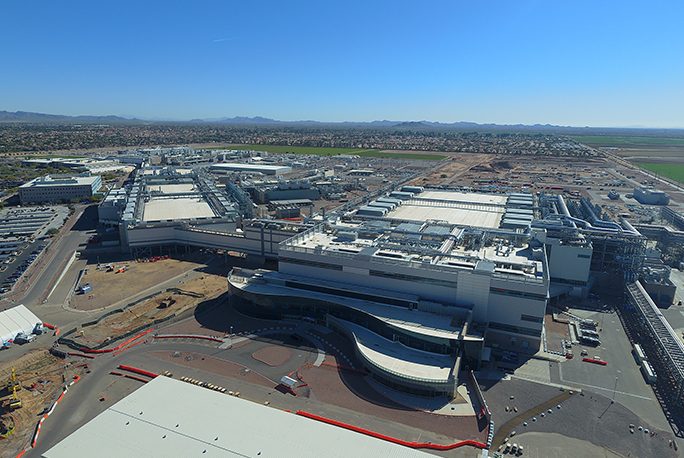
To accelerate Intel’s IDM 2.0 strategy, Gelsinger announced a significant expansion of Intel’s manufacturing capacity, beginning with plans for two new fabs in Arizona, located at the company’s Ocotillo campus. These fabs will support the increasing requirements of Intel’s current products and customers, as well as provide committed capacity for foundry customers.
This build-out represents an investment of approximately $20 billion, which is expected to create over 3,000 permanent high-tech, high-wage jobs; over 3,000 construction jobs; and approximately 15,000 local long-term jobs.
Intel plans to engage the technology ecosystem and industry partners to deliver on its IDM 2.0 vision. To that end, Intel and IBM announced plans for an important research collaboration focused on creating next generation logic and packaging technologies. For more than 50 years, the two companies have shared a deep commitment to scientific research, world-class engineering and a focus on bringing advanced semiconductor technologies to market. These foundational technologies will help unleash the potential of data and advanced computation to create immense economic value.
Leveraging each company’s capabilities and talent in Hillsboro, Oregon, and Albany, New York, this collaboration aims to accelerate semiconductor manufacturing innovation across the ecosystem, enhance the competitiveness of the U.S. semiconductor industry and support key U.S. government initiatives.
Finally, Intel is bringing back the spirit of its popular Intel Developer Forum event this year with the launch of Intel On, a new industry event series. Gelsinger encouraged technology lovers to join him at this year’s Intel Innovation event planned for October in San Francisco.


Discussion about this post